


PCB Design Services
Advanced
Design Solutions provides a full range of PCB
Layout, Routing and Gerber Artwork Generation
services for various design technologies. We adhere
to Military as well as IPC standards to ensure
accuracy and compliance to "Design For
Manufacturing" guidelines.
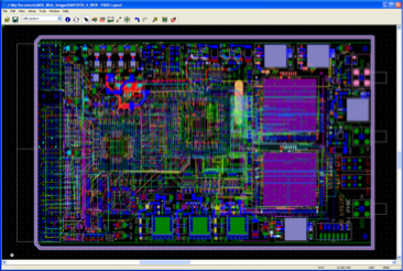
We use the latest state-of-the-art design tools and methodologies to provide you with design solutions. More and more designs require smaller board sizes, smaller component sizes, higher component pin counts and faster speeds. Ball Grid Arrays and High-Density Quad Flat Packs are the norm for board designs these days. This not only poses challenges for PCB layout and routing, but board fabrication and assembly as well. This trend will only continue as customers try to pack as much functionality into the smallest areas possible.
Since we provide full value-added services, we look at the big picture. We work with our fabrication and assembly partners to ensure that our designs will yield the highest quality and help keep costs down. We also keep up with the latest advances in board fabrication and assembly techniques.
- Rigid, Rigid-Flex and Flex PCB's
- CompactPCI, VME, Backplanes, Custom Formats
- High Speed Digital, ECL, RF and Analog
- Ball Grid Arrays, Multi Chip Modules, Fine Pitch Devices
- High Speed Design Rules
- Controlled Impedances (Single-Ended & Differential)
- Single-Sided / Double-Sided Surface Mount
- Blind and Buried Vias, Micro Vias, Via-In-Pad
- Design For Manufacturability (DFM)
- Layer Reduction for better cost control
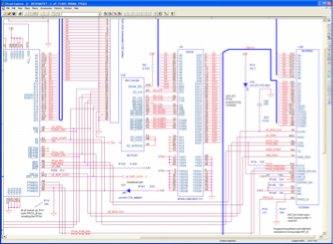
- Orcad® /DXDesigner Schematic Tools
- Mentor PADS Layout®
- Altium Designer®
- Allegro Specctra™ Shape-Based Router
- CAM-350® Gerber Editing Tools
- HyperLnyx®
- AutoCAD ®
We design
state-of-the art circuit boards for AT&T,
General Atomics, Lockheed Martin, Northrop Grumman,
Raytheon, Sandia National Labs and others.
Don't
just think we do name tossing, references are
available upon request.